Light will power the world.
With 3D-integrated photonic chips.
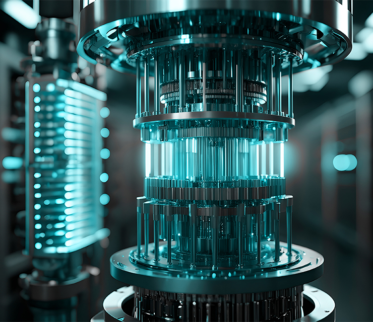
Lightspring enables high-performance, scalable photonic integration with 3D lithography—bridging the gap between design and fabrication for datacom, sensing, and next-gen computing.
Reinventing Photonic Integration
“Our augmented 3D lithography technology is the first to combine optical performance and scalability. We are freeing designers from traditional assembly-related hurdles to turn bold ideas into reality, without compromise.”
Key Expertise - WHAT MAKES US UNIQUE
SOFTWARE-DRIVEN 3D DESIGN
We go beyond 3D CAD and design for optical performance, fabrication efficiency, and reliability.
FULL CONTROL OF OPTICAL MODES
Precise coupling functions and mode control across complex 3D waveguide networks.
FABRICATION SPEED & RELIABILITY
Rapid iteration cycles with repeatable, production-grade quality.
Key Features - BENEFITS FOR CUSTOMERS
PRECISION
0.1 - micron resolution for complex 3D geometries.
Unmatched dimensional accuracy for the most demanding photonic design
SPEED
Iterate in days, not months.
Accelerate time-to-market with rapid prototyping and design validation.
SCALABILITY
From prototyping to production.
Future-ready process that grows from single units to volume manufacturing.
Transforming Industries
with 3D Photonics

Faster, High-Capacity Optical Interconnects
Our 3D lithography process delivers low-loss, high-density couplers and waveguides, optimized for telecom and datacom applications. Achieve higher bandwidth, lower latency, and seamless integration—without the constraints of traditional assembly.
- High-performance fiber-to-chip coupling
- Reduced signal loss and latency
- Scalable for next-gen networks
Precision Sensing, Redefined
Our 3D lithography process delivers low-loss, high-density couplers and waveguides, optimized for telecom and datacom applications. Achieve higher bandwidth, lower latency, and seamless integration—without the constraints of traditional assembly.
- Fast prototyping for sensor development
- Compact, high-precision 3D structures
- Cost-efficient customization

Powering the Next Generation of Computing
From specialized optical interconnects for AI accelerators to quantum chip packaging, our technology enables the high-capacity, low-latency designs that define the future of computing.
- Chiplet integration for AI accelerators
- Quantum computing interconnects
- Scalable 3D photonic architectures
Ready to transform your photonic designs?
Meet the team
Born from world-class photonics research, backed by global innovation networks, and built by engineers who understand what it takes to bring 3D photonics from lab to production.


SUPPORTED BY
